Inside the Avenger KSC321S-2 LNBF
The white plastic cover of the front of the FNBF just pulls off. However it really doesn't want to be removed, so be prepared to struggle with it! There's no simple way to get the two halves of the black plastic cover apart. The two halves clip together internally. The cover is not really intended to be taken off easily. Gentle prying apart is what is required. Once you've popped the black plastic cover off the Avenger KSC321S-2 you will see a number of screws holding the aluminum cover on the body. These are not Phillips head screws but rather (at least on the examples I've seen) Torx head screws, size T8. There's also lots of white caulk which seals the cover to the body. The cover just lifts off (with a little help), breaking the caulk seal, revealing the circuit board inside.
Here's a look at the circuit board inside the Avenger KSC321S-2 LNBF [Available on eBay]
There are separate 1st LNA stages for horizontal and vertical waveguide probes. Which ever one is activated by the power management IC feeds it's output to the common 2nd LNA stage, which in turn feeds its output into the Mixer/Synthesizer/IF amplifier chip. The largest component on the board is the 25Mhz crystal which provides the Mixer/Synthesizer/IF amplifier chip with its frequency reference signal. It's very likely the LNA stages are not optimized at 10.368GHz. The input microstrip dimensions, which would control matching, are probably designed to give optimum performance up around 11.7GHz.
The PC board can be removed by unsoldering the output connector (center of the right hand edge) from the PCB. The under-side of the board is shown below:
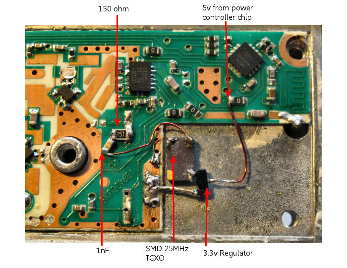
An external reference signal can be injected by removing the 25MHz crystal from the board, installing an SMA connector in the space to the right of it, and connecting the SMA connector to the PC trace as shown, via a 150 ohm resistor in series with a 1000pF (1nF) capacitor (though these values are not at all critical). A few mW at ~25Mhz seems to be about the right level. The 25MHz crystal is a little stubborn, but it will come off if you heat the plated through connections on the under side of the board, while pulling on the crystal.
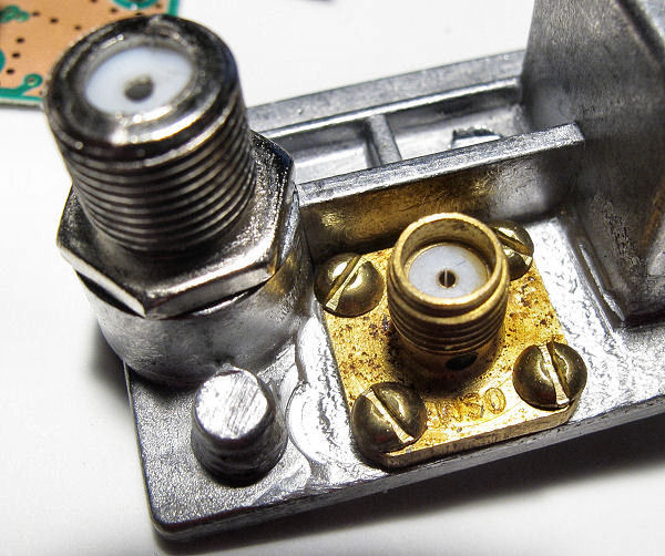
The SMA connector is installed next to the F connector as shown below. It is necessary to remove the aluminum "ribs" on the LNBF housing in order to have a plat area in which to install the connector. This can be done will a mill, a file or probably most easily by a Dremmel type rotary tool. The 4 hold for attaching the SMA panel mount connector are drilled and tapped 2-56.

In theory you could probably run the 25MHz signal up the F connector cable which carries the power to the LNBF and the IF signal back from the LNBF. You'd need some sort of diplexer to separate the 25Mhz signal from the 432/618MHz IF signal, but it could probably be done. Using a separate cable is probably easier though and that's the way I did it. You can also replace the crystal with a miniature TCXO (temperature compensated crystal oscillator), which would improve stability, but being outside in the LNBF enclosure would still be subject to some degree of temperature induced drift. It might reduce drift from 300KHz to 30Khz or maybe even 3kHz, but that's still an excessive amount of frequency drift. If you did use a TCXO it would be better placed indoors where the temperature is more stable, and the signal sent to the LNBF via a cable. Short term stability would probably be good enough to see 10Ghz EME signals, but decoding (which requires better than 10Hz stability over the course of a 48 second transmission), might be compromised.
Any 25MHz TCXO chip should work. The one I used was a Fox924B-25. NOTE: Looking more closely at the output from this TCXO, it seems to frequency hop in very small increments (~ 1Hz) when it drifts too far from 25.000000 MHz. This results in frequency hops of ~400Hz at 10Ghz. It seems to do this mostly on startup while things are warming up and the frequency of the internal crystal would be changing rapidly. After a while it settles down and only occasionally makes a step frequency change. It does hold 25.000000 +/- a few Hz quite well so long term frequency stability is good, but the frequency hops can be annoying. All of this is probably the results of a TCXO using "digitally controlled analog compensation", a technology used in many (most? all?) miniature SMD TCXOs
Since it's a 3.3v device a miniature SMD 3.3v regulator (XC6206) was also required. Here's what an internal TCXO installation looks like:

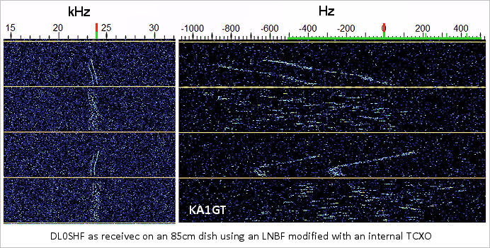
Here's what you might expect to see with such a conversion and an 85cm dish after everything has warmed up to a stable internal temperature. MAP65 was used with a FunCube Dongle tunes to 618 MHz.

Though you can see the traces, there's obviously a loy of drift. A small part of the right to left drift is due to Doppler shift changing at maybe 60 Hz/min, but there's a lot more random drift on top of that. Even if you could tract the nominal Rx frequency to compensate for Doppler changes, you still would not be able to decode this signal.
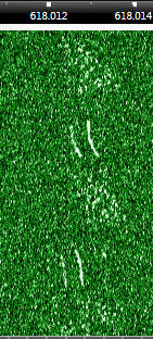
With the FunCube Dongle and SDR-Console tuned to 618MHz the waterfall trace shown below was obtained. The CW and QRA64D tones were just audible.

I would NOT recommend using an internal TCXO for anything more than simple initial experiments. It's much better to use an external frequency reference which you can keep indoors. It can then be at a stable temperature if it's a TCXO or easily change for a more stable source such as one based on an OCXO or GPS stabilized oscillator. To decode any EME signals you will need both a stabilized reference and the ability to track Doppler.
NEXT: Tuning the (modified) LNBF for best system performance
.jpg)